South China Morning Post
ASML EUV in China? The rumour is ridiculed but it reveals a tougher reality on the ground
For anyone closely watching the semiconductor industry, the recent saga around ASML’s denial of possible EUV (extreme ultraviolet) lithography shipments to China, in an apparent response to US concern, may sound almost absurd at first.
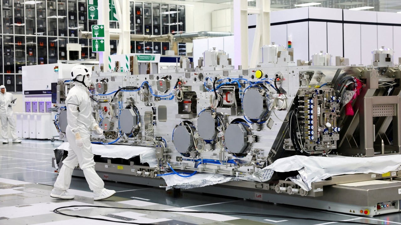
The machine at the centre of the discussion is not a laptop-sized piece of equipment that can be easily packed into a shipping carton. ASML’s EUV lithography systems weigh about 180 tonnes, contain a vast number of precision components, are shipped to customers in the bellies of huge cargo planes, and require extensive installation, calibration and service support.
That is why US Secretary of Commerce Howard Lutnick’s reported concern that such technology may have reached China was met with scepticism, and even ridicule, by some industry observers.
ASML has categorically denied that it shipped any EUV system, or components specifically designed for one, to China. But the episode points to a more serious question for China’s chip industry: if EUV remains out of reach, and access to the most advanced DUV (deep ultraviolet) lithography tools is also tightening, how far can domestic chipmakers progress by relying on older equipment and alternative approaches?
The answer matters because lithography is one of the biggest bottlenecks to China’s semiconductor ambitions. Without ASML’s most advanced tools, Chinese foundries are trying to push DUV multi-patterning further, the country’s tool makers are trying to build domestic lithography systems, while others are exploring new approaches such as advanced packaging, system-level optimisation and Huawei Technologies’ Tau Law.
What is the difference between DUV and EUV?
DUV and EUV refer to different wavelengths of light used in lithography.
View original source — South China Morning Post ↗
Related stories
ABC News
TechnologyJun 24, 2026 · 1 min
Matt Wright sued for negligence after airboat allegedly crashed into tree
ABC News

Philippine Daily Inquirer
TechnologyJun 24, 2026 · 1 min
Cristiano Ronaldo becomes first player to score in six World Cups
Philippine Daily Inquirer

CNA
TechnologyJun 24, 2026 · 1 min
K-pop group Stray Kids announces Singapore stop on Run It world tour and new album This & That
CNA

TechRadar
TechnologyJun 24, 2026 · 1 min
Don’t overspend on your mobile plan — these 5 EOFY deals on SIM-only plans will give you more data for less
TechRadar