The Next Web
Tower Semiconductor puts $3bn into Japan, and Tokyo is paying for a third of it
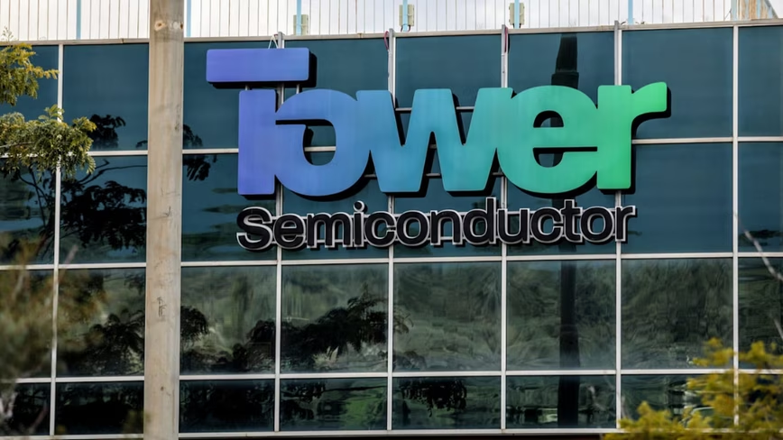
Tower Semiconductor said on Tuesday it will spend roughly $3bn expanding its 300mm operations in Japan, net of about $1bn in grants from the Japanese government, in a two-track build-out aimed squarely at the optical components that AI data centres are consuming faster than anyone can make them.
The announcement, made with the backing of Japan’s Ministry of Economy, Trade and Industry, covers silicon photonics, silicon germanium, and advanced optical packaging.
Tower is a specialist analog foundry rather than a logic manufacturer, which means it does not compete with TSMC for leading-edge nodes. It competes for the plumbing.
Track one repurposes the Arai facility, formerly Fab 6, for 300mm silicon photonics and packaging while pushing output at Fab 7 in Uozu to its maximum.
Full production readiness is expected in the fourth quarter of 2027. On the strength of that alone, Tower raised its 2028 model to $3.6bn of revenue and $1.2bn of net profit.
Track two is the larger bet and the vaguer one. It involves building an entirely new 300mm plant next to Fab 7, subject to the signing and closing of agreements Tower has not detailed, and is expected to deliver what the company calls a multi-fold increase in silicon photonics and silicon germanium capacity.
Tower says it should be “highly accretive” from 2029. Reports of the wider Japanese restructuring have put the eventual combined 300mm capacity at around four times the current Uozu level, though that figure sits outside Tuesday’s release and should be treated as an indication rather than a commitment.
The Japanese assets came to Tower through TPSCo, the joint venture built out of Panasonic’s old semiconductor operations, in which it holds 51%.
Under a separately announced restructuring, Tower is taking full ownership of the 300mm Fab 7 while its partner takes the 200mm site, a tidying-up that makes a $3bn commitment considerably easier to justify to a board.
Chief executive Russell Ellwanger framed the whole thing as an industrial-policy partnership.
“We are honored and appreciative that the Government of Japan has selected Tower to lead the expansion of these strategically important technologies,” he said, invoking Toyama and Niigata prefectures, local suppliers, and Japanese universities in a passage that reads like it was drafted with METI in the room.
The underlying demand story is real enough. Copper interconnects run out of headroom as data rates climb, and once an AI training cluster spans more racks than a short cable can serve, light becomes the only sensible medium.
That is why Nvidia has committed at least $6.5bn to photonics since March, why HyperLight pulled in $80mn for thin-film lithium niobate, and why Tower and Marvell announced in June that they had shipped more than five million coherent photonic ICs between them.
The grant is the other half of the story. Japan has spent the past three years buying its way back into advanced manufacturing, and $1bn of public money to an Israeli foundry, in exchange for a photonics centre of excellence on Japanese soil, is the same trade Europe made when Infineon opened its €5bn Dresden fab under the EU Chips Act. Tokyo is not subsidising chips. It is subsidising presence.
What could go wrong is written into Tower’s own risk language: construction delays, equipment lead times, permits, the negotiation of definitive agreements, and the terms of the METI grants themselves, which the company notes could result in the loss of some or all of the funds if covenants are not met. Track two, notably, has not been signed.
Nor is the input side settled. Beijing has been tightening its checks on indium phosphide, a compound the optical chips inside AI data centres depend on, which is a reminder that capacity is only as useful as the materials feeding it.
Tower has already flagged its second-quarter earnings call, which is the next point at which any of these numbers gets tested against something other than a press release.
View original source — The Next Web ↗
Related stories

Lovin Malta
TechnologyJul 14, 2026 · 1 min
Police Warn Of WhatsApp Scam Hijacking Accounts Through Fake Voting Links
Lovin Malta
Engadget
TechnologyJul 14, 2026 · 1 min
What's the difference between active noise canceling and passive?
Engadget

ZDNet
TechnologyJul 14, 2026 · 1 min
How to install the MacOS 27 public beta on your Mac today - it's live now
ZDNet

Indian Express
TechnologyJul 14, 2026 · 1 min
‘Rs 7 lakh won’t bring justice’: Mumbai Mayor rejects BMC clean chit in Chembur tree death
Indian Express