Indian Express
IBM introduces the world’s first ever sub-1 nanometre chip technology
3 min readNew DelhiJun 25, 2026 05:22 PM IST
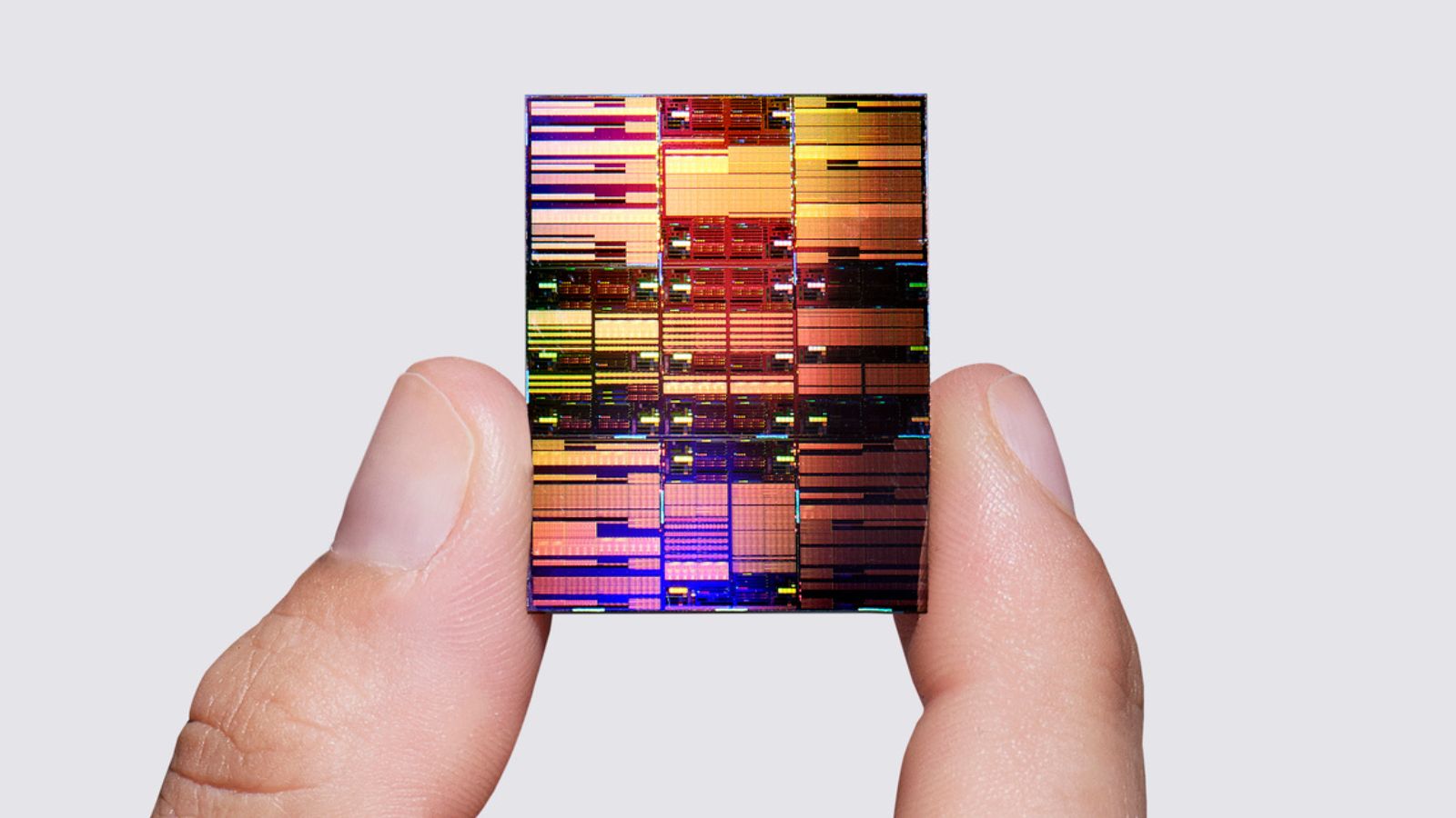
Built with revolutionary “nanostack” 3D chip architecture, IBM’s sub-1 nm chip will propel the semiconductor industry forward for the next decade. (Express Image)
IBM on Thursday, June 25, announced a major breakthrough in semiconductor technology. The tech giant has unveiled what it describes as the world’s first sub-1 nanometer (nm) chip technology featuring a transistor architecture at the 0.7 nm or 7 angstrom node. The company claims that it is a landmark moment as the industry is facing physical constraints in traditional chip scaling.
“IBM’s latest chip breakthrough marks a landmark moment in computing, pushing technology beyond the nanometer era to the scale of atoms. With our new nanostack architecture, we’re not just making smaller transistors, we’re reinventing how chips are built to deliver dramatically more power and energy efficiency,” said Jay Gambetta, Director of IBM Research and IBM Fellow.
Rapid advancements in technology have made semiconductors a crucial component. They play a key role in everything ranging from computing, appliances, to communications equipment, transportation systems, and critical infrastructure. “This industry-first innovation continues IBM’s legacy of leading in next-generation technologies and sets the foundation for the next era of computing,” said Gambetta.
The new sub-1 nm chip comes with around 100 billion transistors all packed into the size of a fingernail. It has nearly twice the density of IBM’s 2nm chip which was launched in 2021. According to the company, the new chip is backed by a range of structural and material innovations, including IBM’s groundbreaking three-dimensional nanostack architecture. The chip shows how regardless of performance and efficiency gains are still possible despite the dimensions.
Further, IBM said that based on published technical results, the new chip is projected to offer a substantial leap in capability, essentially up to 50 per cent more performance. When compared to IBM’s 2 nm node chops, the new chip offers 70 per cent greater energy efficiency meaning it could supercharge compute for applications from generative AI and cloud infrastructure to next-gen electronic devices.
Researchers at IBM created a new transistor architecture called ‘nanostack’, also the industry’s first known three-dimensional and nanosheet-based design, to develop the new chip. While nanosheet technology is currently the leading-edge architecture invented by IBM, the new nanostack is an advancement far beyond it.
The architecture essentially stacks and staggers transistors vertically with the help of 3D sequential integration to include more transistors onto a chip. This type of architecture also allows for the use of different material combinations within each stacked layer which optimises performance and power efficiency of each transistor independent from the other.
View original source — Indian Express ↗
Related stories

Portugal Resident
TechnologyJun 25, 2026 · 1 min
The summer Milky Way is now overhead in July evenings
Portugal Resident

Indian Express
TechnologyJun 25, 2026 · 1 min
Maharashtra Assembly orders SIT in Lohagad fort fiancee murder case
Indian Express

TechRadar
TechnologyJun 25, 2026 · 1 min
How banks can build a risk-intelligent approach to core modernization
TechRadar

The Next Web
TechnologyJun 25, 2026 · 1 min
Cannes insights: What a two-time major champion knows about marketing that CMOs don’t
The Next Web